
파일:Wafer flats convention v2.svg

SVG 파일의 PNG 형식의 미리보기 크기: 150 × 150 픽셀. 다른 해상도: 240 × 240 픽셀 | 480 × 480 픽셀 | 768 × 768 픽셀 | 1,024 × 1,024 픽셀 | 2,048 × 2,048 픽셀
원본 파일 (SVG 파일, 실제 크기 150 × 150 픽셀, 파일 크기: 13 KB)
파일 설명
| 설명 |
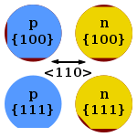
Wafer flats convention, based on Image:Wafer flats convention.PNG Conventional meaning of flats in semiconductor wafers. Red denotes material that has been removed. Wafer orientation is the orientation of the crystallographic plane in which the crystal grew. Wafer type indicated the type of doping.
|
| 날짜 | |
| 출처 |
self-made, |
| 저자 | Twisp |
| 다른 버전 | Wafer flats convention.PNG |
라이선스
| 나는 이 작품의 저작권자로서, 이 작품을 퍼블릭 도메인으로 모두에게 공개합니다. 이 공개 선언은 전 세계적으로 유효합니다. 만약 저작권의 포기가 법률적으로 가능하지 않은 경우, 나는 이 작품을 법적으로 허용되는 한도 내에서 누구나 자유롭게 어떤 목적으로도 제한없이 사용할 수 있도록 허용합니다. |
파일 역사
날짜/시간 링크를 클릭하면 해당 시간의 파일을 볼 수 있습니다.
| 날짜/시간 | 섬네일 | 크기 | 사용자 | 설명 | |
|---|---|---|---|---|---|
| 현재 | 2013년 9월 25일 (수) 06:40 | | 150 × 150 (13 KB) | Cepheiden | fixed position of secondary flat Silicon processing for the VLSI era - Vol. 1 - Process technology; S Wolf; RN Tauber - Lattice Press; 1986; ISBN 096167237; p. 23 |
| 2008년 12월 23일 (화) 09:37 |  | 150 × 150 (13 KB) | Inductiveload | Added arrow indication <110> direction and enlarged flats so they can be easily seen | |
| 2008년 3월 1일 (토) 06:17 |  | 150 × 150 (9 KB) | Twisp | ||
| 2008년 3월 1일 (토) 06:13 |  | 150 × 150 (9 KB) | Twisp | ||
| 2008년 3월 1일 (토) 06:06 |  | 150 × 150 (8 KB) | Twisp | ||
| 2008년 3월 1일 (토) 05:59 |  | 150 × 150 (8 KB) | Twisp | ||
| 2008년 3월 1일 (토) 03:09 |  | 150 × 150 (9 KB) | Twisp | {{Information |Description= Wafer flats convention, based on Image:Wafer flats convention.PNG Conventional meaning of ''flats'' in semiconductor wafers. Black denotes material that has been removed. Wafer orientation is |
이 파일을 사용하는 문서
다음 문서 1개가 이 파일을 사용하고 있습니다:
이 파일을 사용하고 있는 모든 위키의 문서 목록
다음 위키에서 이 파일을 사용하고 있습니다:
- ca.wikipedia.org에서 이 파일을 사용하고 있는 문서 목록
- cs.wikipedia.org에서 이 파일을 사용하고 있는 문서 목록
- de.wikipedia.org에서 이 파일을 사용하고 있는 문서 목록
- en.wikipedia.org에서 이 파일을 사용하고 있는 문서 목록
- es.wikipedia.org에서 이 파일을 사용하고 있는 문서 목록
- et.wikipedia.org에서 이 파일을 사용하고 있는 문서 목록
- eu.wikipedia.org에서 이 파일을 사용하고 있는 문서 목록
- fi.wikipedia.org에서 이 파일을 사용하고 있는 문서 목록
- it.wikipedia.org에서 이 파일을 사용하고 있는 문서 목록
- it.wikibooks.org에서 이 파일을 사용하고 있는 문서 목록
- ja.wikipedia.org에서 이 파일을 사용하고 있는 문서 목록
- nl.wikipedia.org에서 이 파일을 사용하고 있는 문서 목록
- pl.wikipedia.org에서 이 파일을 사용하고 있는 문서 목록
- ro.wikipedia.org에서 이 파일을 사용하고 있는 문서 목록
- sk.wikipedia.org에서 이 파일을 사용하고 있는 문서 목록
- uk.wikipedia.org에서 이 파일을 사용하고 있는 문서 목록
- www.wikidata.org에서 이 파일을 사용하고 있는 문서 목록