
파일:Bankswitch memory map.svg

SVG 파일의 PNG 형식의 미리보기 크기: 463 × 599 픽셀. 다른 해상도: 185 × 240 픽셀 | 371 × 480 픽셀 | 593 × 768 픽셀 | 791 × 1,024 픽셀 | 1,582 × 2,048 픽셀 | 765 × 990 픽셀
원본 파일 (SVG 파일, 실제 크기 765 × 990 픽셀, 파일 크기: 31 KB)
파일 설명
| 설명 |
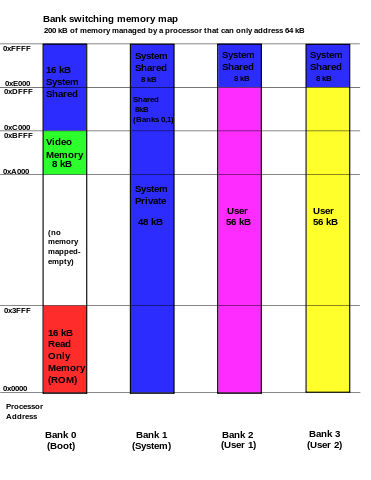
English: A hypothetical bank switching memory map showing how a processor that can only address 64 kB could have 200 kB of memory connected. In this hypothetical system, the processor would start with Bank 0 only active, then would switch between banks 0, 1, 2 and 3 depending on the needs of the operating system or users. Code to switch between banks must be kept above 0xE000 address, otherwise a transition between banks would be one-way only. When 8-bit processors were common in desktop computers, each logical bank of memory might well have been a discrete set of physical memory chips. |
| 날짜 | (UTC) |
| 출처 | 자작 (Original text: I (Wtshymanski (talk)) created this work entirely by myself.) |
| 저자 | Wtshymanski (talk) |
라이선스
영어 위키백과의 Wtshymanski은(는) 아래 작품의 저작권자로서, 해당 저작물을 다음과 같은 라이선스로 배포합니다.
이 파일은 크리에이티브 커먼즈 저작자표시-동일조건변경허락 3.0 Unported 라이선스로 배포됩니다.
저작자표시: 영어 위키백과의 Wtshymanski
- 이용자는 다음의 권리를 갖습니다:
- 공유 및 이용 – 저작물의 복제, 배포, 전시, 공연 및 공중송신
- 재창작 – 저작물의 개작, 수정, 2차적저작물 창작
- 다음과 같은 조건을 따라야 합니다:
- 저작자표시 – 적절한 저작자 표시를 제공하고, 라이센스에 대한 링크를 제공하고, 변경사항이 있는지를 표시해야 합니다. 당신은 합리적인 방식으로 표시할 수 있지만, 어떤 방식으로든 사용권 허가자가 당신 또는 당신의 사용을 지지하는 방식으로 표시할 수 없습니다.
- 동일조건변경허락 – 만약 당신이 이 저작물을 리믹스 또는 변형하거나 이 저작물을 기반으로 제작하는 경우, 당신은 당신의 기여물을 원저작물과 동일하거나 호환 가능한 라이선스에 따라 배포하여야 합니다.

|
GNU 자유 문서 사용 허가서 1.2판 또는 자유 소프트웨어 재단에서 발행한 이후 판의 규정에 따라 본 문서를 복제하거나 개작 및 배포할 수 있습니다. 본 문서에는 변경 불가 부분이 없으며, 앞 표지 구절과 뒷 표지 구절도 없습니다. 본 사용 허가서의 전체 내용은 GNU 자유 문서 사용 허가서 부분에 포함되어 있습니다. |
이 라이선스 중에서 목적에 맞는 것을 선택하여 사용할 수 있습니다.
기존 올리기 기록
Wdwd 사용자가 CommonsHelper 도구를 사용하여 en.wikipedia에서 공용으로 옮겨왔습니다.
The original description page was here. All following user names refer to en.wikipedia.
- 2010-03-27 02:02 Wtshymanski 765×990× (31845 bytes) {{Information |Description = A hypothetical bank switching memory map showing how a processor that can only address 64 kB could have 200 kB of memory connected. In this hypothetical system, the processor would start with Bank 0 only active, then would
파일 역사
날짜/시간 링크를 클릭하면 해당 시간의 파일을 볼 수 있습니다.
| 날짜/시간 | 섬네일 | 크기 | 사용자 | 설명 | |
|---|---|---|---|---|---|
| 현재 | 2011년 6월 13일 (월) 06:03 | | 765 × 990 (31 KB) | File Upload Bot (Magnus Manske) | {{BotMoveToCommons|en.wikipedia|year={{subst:CURRENTYEAR}}|month={{subst:CURRENTMONTHNAME}}|day={{subst:CURRENTDAY}}}} {{Information |Description={{en|A hypothetical bank switching memory map showing how a processor that can only address 64 kB could have |
이 파일을 사용하는 문서
다음 문서 1개가 이 파일을 사용하고 있습니다:
이 파일을 사용하고 있는 모든 위키의 문서 목록
다음 위키에서 이 파일을 사용하고 있습니다:
- az.wikipedia.org에서 이 파일을 사용하고 있는 문서 목록
- ca.wikipedia.org에서 이 파일을 사용하고 있는 문서 목록
- de.wikipedia.org에서 이 파일을 사용하고 있는 문서 목록
- en.wikipedia.org에서 이 파일을 사용하고 있는 문서 목록
- en.wikibooks.org에서 이 파일을 사용하고 있는 문서 목록
- id.wikipedia.org에서 이 파일을 사용하고 있는 문서 목록
- nl.wikipedia.org에서 이 파일을 사용하고 있는 문서 목록
- ru.wikipedia.org에서 이 파일을 사용하고 있는 문서 목록
- uk.wikipedia.org에서 이 파일을 사용하고 있는 문서 목록